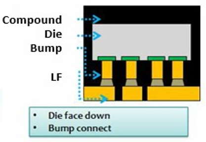
Product Introduction
The full name of FCDFN is Flip Chip Dual Flat No Leads, which literally means dual planar no pin flip.
Product Features
Good heat dissipation performance
The large-area solder pads at the bottom of the chip can be directly adhered to the PCB, and heat can be quickly conducted to the PCB, and then dissipated through the heat dissipation copper foil, heat sink and other structures on the PCB, forming an efficient heat dissipation channel. Compared with traditional packaging, it can more effectively reduce the working temperature of the chip and ensure its stability during high load operation.
Superior electrical performance
The pinless design avoids the additional inductance and capacitance caused by pins, and the signal transmission path is simple and direct. When transmitting high-frequency and high-speed signals, it can effectively reduce signal attenuation and delay, ensure data integrity and accuracy, and meet the strict requirements for electrical performance in applications such as 5G communication and high-speed data storage.
application
Smart phone, smart watch, Bluetooth headset, automobile power system, auto drive system, etc.
process characteristics
High precision inverted mounting
In a dust-free, constant temperature, and constant humidity ultra clean environment, high-precision equipment is used to accurately flip the chip onto the substrate. Inverted chip technology requires extremely high process control, ensuring that the alignment accuracy between the chip and the substrate reaches the micrometer level or even higher, in order to achieve reliable electrical connections and mechanical stability. For example, in the process of producing bumps, it is necessary to precisely control the height, shape, and position of the bumps, as well as the alignment accuracy between the chip and the substrate. Any small deviation may affect product performance.
Pin free packaging structure
This packaging form reduces parasitic parameters such as inductance and capacitance caused by pins, reduces signal transmission delay and distortion, and improves electrical performance. At the same time, the pinless structure also makes the packaging more compact, reducing the packaging size and facilitating the miniaturization and high-density integration of electronic products. For example, in applications of high-frequency and high-speed signal transmission, pinless packaging can effectively reduce signal reflection and crosstalk, and improve signal integrity.
Precision substrate and pad design
The substrate is usually made of materials with good mechanical and electrical properties, such as ceramics, glass fiber reinforced plastics, etc., to provide stable support and insulation performance. The design of solder pads needs to consider factors such as compatibility with chip solder joints, reliability of electrical connections, and heat dissipation performance. For example, the size, shape, and spacing of the solder pads need to be carefully designed to ensure good bonding with the chip solder joints, while increasing the area of the solder pads can improve heat dissipation efficiency.